
Carbonics has announced its Zebra carbon-on-silicon wafers, which integrate radio frequencies on CMOS system-on-chip (SoC). In a bid to make the move to 5G less costly and efficient, the company has created wafers that allow fabrication of high-speed functions along with complementary metal oxide semiconductors (CMOS).
“Our technology is kick ass for high frequency RF and CMOS compatibility,” Carbonics’ CEO Kos Galatsis said. “Our wafer technology is where the business opportunities are. For instance, WiGig, is growing at a rate of 30 percent per year and our wafers are perfect for it.”
Carbon-coated silicon wafers could also be a real boon to today’s cell phones, but will shine during the move to 5G, which will operate at higher frequencies than 4G.
Many methods have been invented to deposit parallel carbon nanotubes onto silicon wafers, but none have been economically feasible for mass production until now. The advantage of using carbon nanotubes, especially for RF, is its ultra-high electron mobility—a high as 100,000cm2 V-1s-1 compared to 1400cm2 V-1s-1 for silicon and 8500cm2 V-1s-1 for gallium arsenide—the usual medium for RF transistors.
The reason that Carbonics technique is so economical is that it is done at normal temperatures using a solution-based method. The nanotubes are merely mixed into the solution and the silicon wafer then dipped into the solution where they stick to the top of the wafer. Then as the wafer is slowly removed from the solution, it pulls along the nanotubes which automatically align alongside each other. The process can be repeated with the same wafer as many times as needed to achieve the necessary current capability of the RF transistor channel.
After the wafer dries, normal lithographic techniques can be used to form the transistor channels, then the unneeded nanotubes are etched off using an oxygen plasma.
“Our process is very simple. IBM is doing wafers too, but using a very complicated process, with many many steps using die-block co-polymers,” Galatsis explained. “Whereas Carbonics does the whole process in a single step dip-coating in a bath of oil using the magic of surface tension as it raises them out.”
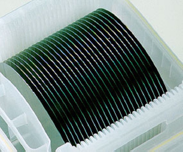
Figure 1: Carbonics’ Zebra carbon-on-silicon wafers contain nanotubes that act as channel for transistors.
Each channel will have the number of tubes required for the necessary current. Carbonics claims it can achieve milliamps per millimetre and microamps per micrometre in channel width, compared to gallium arsenide (GaAs) which achieves only 600µA/mm, according to Galatsis.
The first wafers—called Zebra because of the microscopic nanotube stripes—will be available four-inches in diameter for research and development. The Zebra Bolt will fabricate the nanotubes atop 15nm thick of oxide for backgated applications such as sensors and detectors. The Zebra Sprint will deposit the nanotubes on silicon for top-gated amps, memory, switches and logic. The Zebra Sprint will deposit the nanotubes directly onto quartz for RF applications as high as 100GHz (with terahertz operation slated for the next generation).
Its next product, due later this year, is called Viper will also be for R&D purposes, but will include pre-fabricated RF devices such as integrated power amplifiers (PAs).
Then in 2018, Carbonics plans its Stingray line which will include RFICs and MMICs that will operate in the terahertz range, including mixers switches and complete RF front-end modules by 2019.
Carbonics was spun off from UCLA and KACST Center of Excellence in 2014 and is backed by $5.5 million from Taqnia International.
First published on EE Times.